Definition
A tunnel diode or Esaki diode is a type of semiconductor diode which is capable of very fast operation, well into the microwave region GHz, by utilizing quantum mechanical effects.
Tunnel Diode Basics
The tunnel diode was invented in August 1957 by Leo Esaki when he was with Tokyo Tsushin Kogyo (now known as Sony), who in 1973 received the Nobel Prize in Physics for discovering the electron tunneling effect used in these diodes.
These diodes have a heavily doped p–n junction only some 10 nm (100 Å) wide. The heavy doping results in a broken bandgap, where conduction band electron states on the n-side are more or less aligned with valence band hole states on the p-side.
Tunnel diodes were manufactured by Sony for the first time in 1957 followed by General Electric and other companies from about 1960, and are still made in low volume today. Tunnel diodes are usually made from germanium, but can also be made in gallium arsenide and silicon materials. They can be used as oscillators, amplifiers, frequency converters and detectors.
Forward bias operation
Under normal forward bias operation, as voltage begins to increase, electrons at first tunnel through the very narrow p–n junction barrier because filled electron states in the conduction band on the n-side become aligned with empty valence band hole states on the p-side of the pn junction. As voltage increases further these states become more misaligned and the current drops – this is called negative resistance because current decreases with increasing voltage. As voltage increases yet further, the diode begins to operate as a normal diode, where electrons travel by conduction across the p–n junction, and no longer by tunneling through the p–n junction barrier. Thus the most important operating region for a tunnel diode is the negative resistance region.
Reverse bias operation
When used in the reverse direction they are called back diodes and can act as fast rectifiers with zero offset voltage and extreme linearity for power signals (they have an accurate square law characteristic in the reverse direction).
Under reverse bias filled states on the p-side become increasingly aligned with empty states on the n-side and electrons now tunnel through the pn junction barrier in reverse direction – this is the Zener effect that also occurs in zener diodes.
Technical comparisons
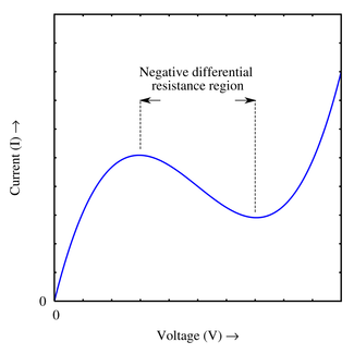
A rough approximation of the VI curve for a tunnel diode, showing the negative differential resistance region
In a conventional semiconductor diode, conduction takes place while the p–n junction is forward biased and blocks current flow when the junction is reverse biased. This occurs up to a point known as the “reverse breakdown voltage” when conduction begins (often accompanied by destruction of the device). In the tunnel diode, the dopant concentration in the p and n layers are increased to the point where the reverse breakdown voltage becomes zero and the diode conducts in the reverse direction. However, when forward-biased, an odd effect occurs called “quantum mechanical tunnelling” which gives rise to a region where an increase in forward voltage is accompanied by a decrease in forward current. This negative resistance region can be exploited in a solid state version of the dynatron oscillator which normally uses a tetrode thermionic valve (or tube).
The tunnel diode showed great promise as an oscillator and high-frequency threshold (trigger) device since it would operate at frequencies far greater than the tetrode would, well into the microwave bands. Applications for tunnel diodes included local oscillators for UHF television tuners, trigger circuits in oscilloscopes, high speed counter circuits, and very fast-rise time pulse generator circuits. The tunnel diode can also be used as low-noise microwave amplifier. However, since its discovery, more conventional semiconductor devices have surpassed its performance using conventional oscillator techniques. For many purposes, a three-terminal device, such as a field-effect transistor, is more flexible than a device with only two terminals. Practical tunnel diodes operate at a few millamperes and a few tenths of a volt, making them low-power devices. The Gunn diode has similar high frequency capability and can handle more power.
Tunnel diodes are also relatively resistant to nuclear radiation, as compared to other diodes. This makes them well suited to higher radiation environments, such as those found in space applications.
Longevity
Esaki diodes are notable for their longevity; devices made in the 1960s still function. Writing in Nature, Esaki and coauthors state that semiconductor devices in general are extremely stable, and suggest that their shelf life should be "infinite" if kept at room temperature. They go on to report that a small-scale test of 50-year-old devices revealed a "gratifying confirmation of the diode's longevity".
Topics of Interest
Resonant tunneling diode (RTD) is a diode with a resonant tunneling structure in which electrons can tunnel through some resonant states at certain energy levels. The current–voltage characteristic often exhibits negative differential resistance regions.
All types of tunneling diodes make use of the quantum mechanical tunneling. Characteristic to the current-voltage relationship of a tunneling diode is the presence of one or more negative differential resistance regions, which enables many unique applications. Tunneling diodes can be very compact and are also capable of ultra high-speed operation because the quantum tunneling effect through the very thin layers is a very fast process.
Source: Wikipedia (All text is available under the terms of the GNU Free Documentation License and Creative Commons Attribution-ShareAlike License.)
|


